Original Link: https://www.anandtech.com/show/1217
Covert Ops in Taiwan - Intel Tejas & Socket 775 Unveiled
by Anand Lal Shimpi on January 9, 2004 10:49 AM EST- Posted in
- CPUs
While the majority of the AnandTech staff was hard at work in Las Vegas covering CES, a quiet staff member was touring the streets of Taipei.
During his visit to Taipei he came across some information shared by some very good contacts about Intel's Prescott successor - Tejas. Very few people caught on to the fact that we actually talked about Tejas on AnandTech years ago as we heard about the codename before Prescott and even before Northwood, hidden in an Intel presentation that hadn't properly been cleaned up. Originally Tejas was listed as the first Intel CPU to have a 1.2GHz FSB, but now we know a bit more about the CPU.
Apparently a total of 10 Tejas samples have been shipped out to various friends of Intel, all running at 2.8GHz. What's also interesting to note is that our sources have informed us that at 2.8GHz Tejas uses around 150W of power - about 50% more than Prescott at the same clock speed.
Given that Tejas is still a 90nm part, it would be unlikely that the additional power consumption would be due to a larger cache as that would make the die huge and isn't Intel's style to increase cache size without shrinking the die further. If the power figures we've been given are indeed correct, one possible explanation would be that Tejas is indeed some variation of a multicore CPU. While it is unlikely that Tejas includes two discrete Prescott cores on die, there is a chance that the two cores (if they exist) could be sharing data caches and maybe other units. A multicore Tejas would explain the jump in power consumption, and it is in line with Intel's strategy although it does seem sooner than expected.
The 10 Tejas samples are all LGA-775 CPUs and luckily our contact was able to gather some pictures of the CPU and the interface so you all can get a glimpse of what is soon to come. We had to blur out some parts of the pictures to protect the identity of our sources, but you'll still be able to see what's important.
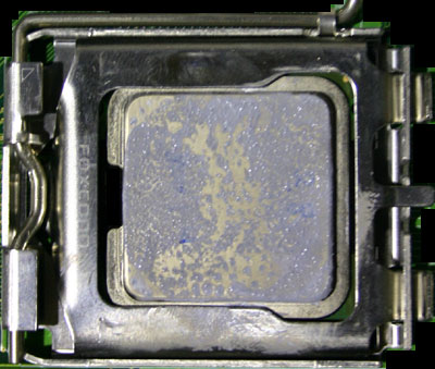
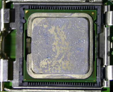
In the shot above you'll see the Tejas as it appears immediately after you remove the heatsink. There is a lever at the top of the picture that you can barely see that will allow you to remove the CPU. Unlatching the lever will result in the picture below. The metal covering can now be pulled up thus exposing the CPU, which can easily be removed:
The notches on either side of the CPU at the top of the picture prevent it from being inserted improperly and also help line up the contact points on the bottom of the CPU.
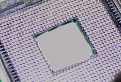
Before we look at the bottom of the CPU itself, let's look at what's underneath the CPU - a bed of pins (note that we purposefully blocked out some of what was in the middle of the pins):
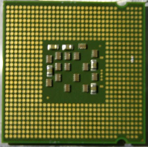
Now to flip the chip over we've got a nice look at the flat surface of the pinless CPU - welcome to LGA-775. This is the same CPU interface that you'll find on Prescott CPUs after April, but what you're looking at here is Tejas as far as we know.
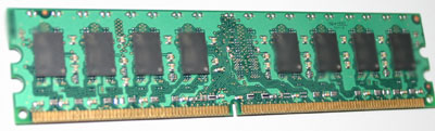
As an added kick here's a DDR-II module out of the Tejas system:
There you have it; no benchmarks, not a lot of information, but some interesting pictures and hopefully something to think about for what happens after Prescott...


