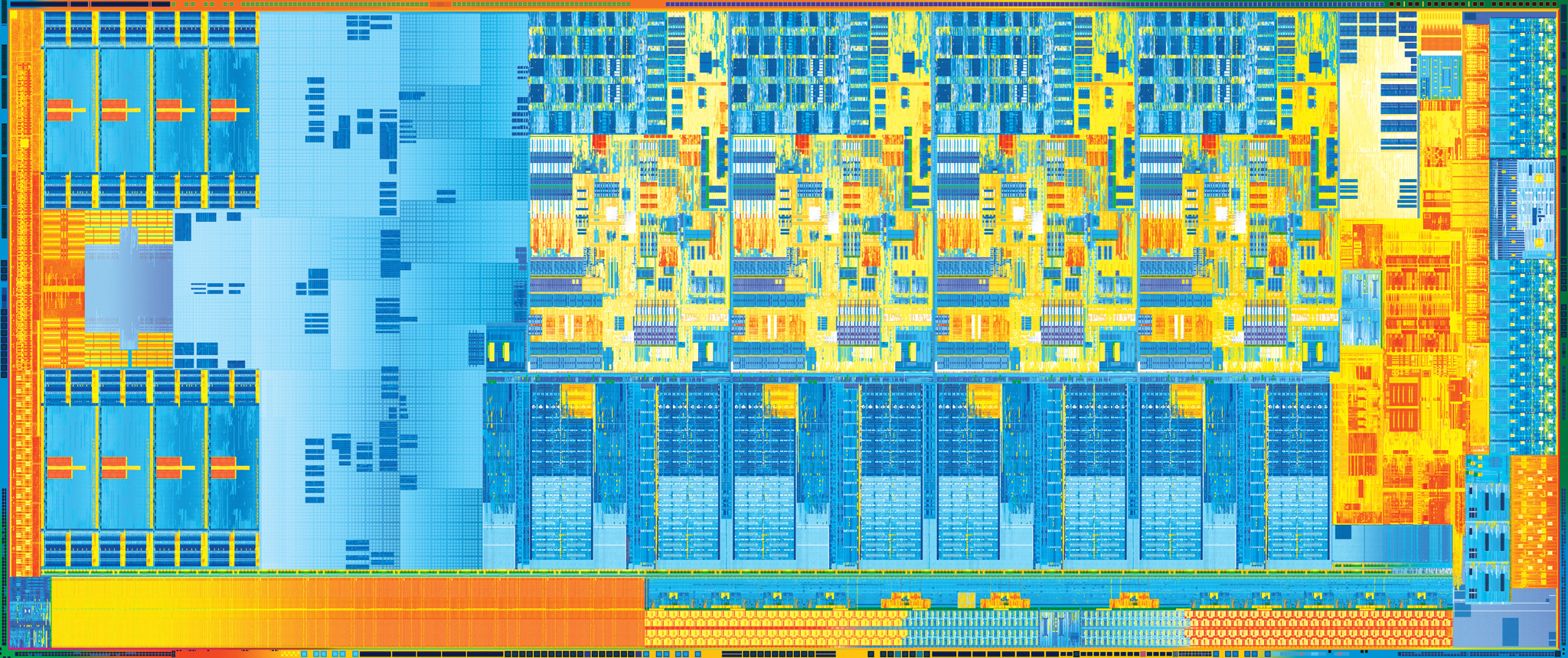
Dual Core/GT2 Ivy Bridge Die Measured: ~121mm^2
by Anand Lal Shimpi on May 31, 2012 2:25 PM EST- Posted in
- CPUs
- Intel
- Ivy Bridge
- Ultrabook
I mentioned Intel's desired secrecy around die sizes and transistor counts for the majority of the Ivy Bridge lineup in our 3470 review from this morning. While I can't count individual transistors in the Core i7-3517U that was in ASUS' Zenbook Prime UX21A we reviewed a week ago, I can measure its exposed die.
Mobile CPUs rarely feature integrated heatspreaders, giving us direct access to the back side of the processor die itself. The dual-core die looks very similar to the quad-core die, it's just not as long. Armed with a pair of digital calipers, I can get a good idea of the CPU's die area.
The die measures approximately 14.7mm x 8.2mm, covering 120.54mm^2 of area. That's roughly 75% of the die area of the quad-core/GT2 Ivy Bridge part:
| CPU Specification Comparison | ||||||||
| CPU | Manufacturing Process | CPU Cores | Transistor Count | Die Size | ||||
| Apple A5R2 | 32nm LP | 2 | ?? | 69mm2 | ||||
| Apple A5X | 45nm LP | 2 | ?? | 163mm2 | ||||
| AMD Bulldozer 8C | 32nm | 8 | 1.2B | 315mm2 | ||||
| Intel Ivy Bridge 2C (GT2) | 22nm | 2 | ?? | 121mm2 | ||||
| Intel Ivy Bridge 4C (GT2) | 22nm | 4 | 1.4B | 160mm2 | ||||
| Intel Sandy Bridge E (6C) | 32nm | 6 | 2.27B | 435mm2 | ||||
| Intel Sandy Bridge E (4C) | 32nm | 4 | 1.27B | 294mm2 | ||||
| Intel Sandy Bridge 4C | 32nm | 4 | 1.16B | 216mm2 | ||||
| Intel Lynnfield 4C | 45nm | 4 | 774M | 296mm2 | ||||
| Intel Sandy Bridge 2C (GT1) | 32nm | 2 | 504M | 131mm2 | ||||
| Intel Sandy Bridge 2C (GT2) | 32nm | 2 | 624M | 149mm2 | ||||
I included the two Apple SoCs to put Intel's 2C/GT2 die size in perspective. It's entirely possible to build very high performance smartphone/tablet class silicon given a modern enough manufacturing process. While I doubt we'll see anything this class in an iPad anytime soon, when we get to Broadwell (14nm Haswell shrink) the tablet market will be very interesting indeed. Haswell is expected to narrow the idle power consumption gap that separates ARM and big x86 silicon, while increasing die size at the high end. Broadwell will bring die area back in check with a move to 14nm.


18 Comments
View All Comments
thunderising - Friday, June 1, 2012 - link
Amazing job on that. It's amazing to even think INTEL is selling 132 mm^2 quad cores at the 300$ price range (non "k" parts I believe).Just in 2007, Core 2 Quad Q6600 had become popular, at 65nm, 4 cores, quite a die size too, it cost the same or lesser I believe (after price cuts).
I was really hoping INTEL bring on more to people. We've been stuck with over-priced quadcores for far too long.
And as we can see, the GT2 Dual Cores are barely much smaller than the GT1 Quad Cores, making the GT2 Duals more and more irrelevant and the Quad's more and more relevant.
Shadowmaster625 - Thursday, May 31, 2012 - link
It costs roughly 2 square mm in die space to add each EU. So why did they stop at 16? Why not release one model with 32 EU? It would still be around the same size its predecessor.stadisticado - Thursday, May 31, 2012 - link
Because no OEMs were willing to pay more for it?Because investors like it when Intel hits GM targets?
Because the vast majority of corporate and even personal users have no need for all those EUs?
Because this might have cause thermal and/or memory bandwidth issues?
Really, take your pick, but my money is with the fact that adding more EUs would not have added revenue in line with the cost of adding them. In which case, they made the correct business decision.
fic2 - Thursday, May 31, 2012 - link
What I don't get is why they didn't add 2 EUs to the 2500 and make it faster than the HD3000. At least then it could have 1/2 the EUs of the HD4000. But to truly "earn" the 2500 name vs the 4000 it should have 10 EUs (2500/4000 = 0.625 * 16 EU = 10).But I guess that Intel has figured out that 6 EUs is good enough for any cpu based graphics and if you need more than that you are going to get a discrete card anyway.
Based on that I don't know why they bother with the HD3000/4000 since they truly just waste die space and energy for no gain.
IntelUser2000 - Friday, June 1, 2012 - link
That's not true. HD 2500 is equal in performance to the HD 3000, but the 2600K tested has higher GPU clocks. It performs the same when compared to the 2500K's HD 3000, which features similar clocks.http://hothardware.com/Reviews/Intel-Core-i53470-Q...
Although HD 2500 has only 6 EUs, the throughput per EUs are doubled, making it equivalent to a 12 EU HD 3000.
fic2 - Friday, June 1, 2012 - link
I didn't realize that the 2500 was equal to the 3000. Thanks for the info.dagamer34 - Thursday, May 31, 2012 - link
Intel didn't think enough OEMs besides Apple would be interested. They don't want to build custom parts.jjj - Thursday, May 31, 2012 - link
"I included the two Apple SoCs to put Intel's 2C/GT2 die size in perspective. It's entirely possible to build very high performance smartphone/tablet class silicon given a modern enough manufacturing process."Extreme simplification there or flawed logic. that sounds like Otellini.
You got to factor in clocks,temps,power, how much of the chip is active at any one time and cost.